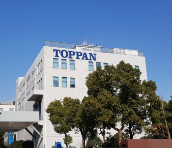
Toppan Printing Co., Ltd. (hereafter Toppan Printing; head office: Chiyoda Ward, Tokyo; President & Representative Director: Shingo Kaneko) will invest in new equipment for the mass production of advanced photomasks at the plant of Toppan Photomasks Company Limited, Shanghai (hereafter TPCS; head office: Shanghai, China; Chairman and Representative Director: Terry W. Russell), a manufacturing subsidiary of Toppan Photomasks Inc. (hereafter TPI; head office: Texas, USA; CEO: Michael G. Hadsell), which produces photomasks for semiconductors. Leading-edge equipment will be introduced and installed by autumn 2018.
Production of 65/55 nm photomasks is scheduled to begin in April 2018, with production of 14 nm photomasks due to be launched during fiscal 2018.

- Background
The global semiconductor market continues to grow due to the enhanced functionality and further miniaturization of devices such as smartphones and IoT equipment. The market is estimated to be worth about \50 trillion in 2018. In China in particular, many semiconductor manufacturers are establishing production bases, which will create strong demand for advanced photomasks and a need for stable supply systems based on local production.
Since entering the photomask business in 1961, Toppan Printing has been a major presence in the sector, boasting industry-leading technologies and supply capabilities. In China, TPCS commenced production in 1995 and installed production equipment for 90 nm photomasks in 2015, contributing to Toppan’s maintaining a leading share of the market.
Introducing cutting-edge equipment to TPCS will now enable an integrated production system for both advanced products and existing standard products, as well as replacement of protective-film (pellicle), which requires short lead times.
- Future targets
With this investment, Toppan Printing will enhance leading-edge photomask production capabilities in China, combine strengths with production bases in Japan and Taiwan, and target sales of approximately \4.5 billion in the Asian market in 2020.
We will continue to produce next-generation semiconductor photomasks for the 10 nm node and beyond, develop cutting-edge products, such as EUV photomasks expected to be adopted from the 7 nm generation, and maintain our competitive advantage in the booming global semiconductor-related market.
* The information in this press release is current as the date of publication and is subject to change without notice.