TOPPAN
Electronics Business Unit
FC-BGA substrates
FC-BGA substrates
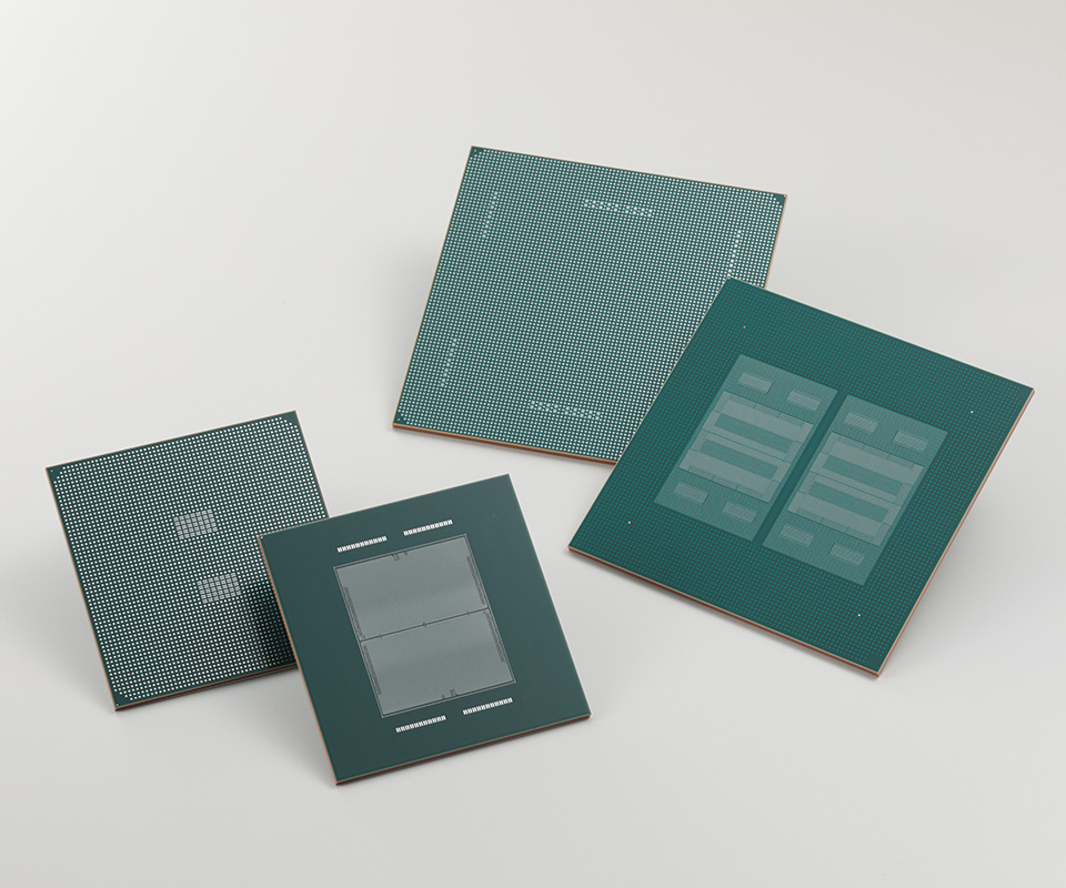
FC-BGA (FCBGA : Flip Chip-Ball Grid Array) on a high density semiconductor package substrate allows high speed LSI chips with more functions.
We have developed ultra high density wiring substrates with our original microfabrication and build-up wiring technologies, offering products supporting current semiconductor microfabrication.
For a growing demand for LSIs for automotive SoC or high-end processors (server, AI, network) as well as for PCs or game devices, we provide comprehensive support from substrate design to production.
Solutions for lead-free and halogen-free products are also available.
Structure & Manufacturing process
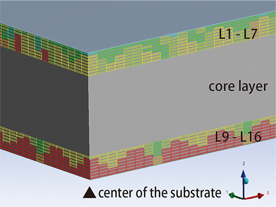
Structure of FC-BGA

Manufacturing process
-
Core Process
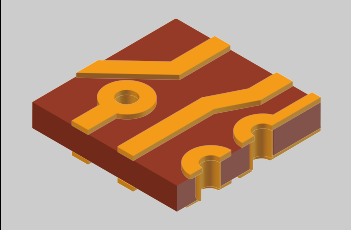
Drill holes in the core material and plate it with copper. Then remove the copper except for a circuit pattern area.
-


-
Build-up processing
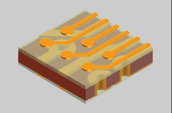
Expose a circuit pattern to directly form circuit with copper plating. Repeat this treatment and laminate (build up)
-


-
Outer layer Process
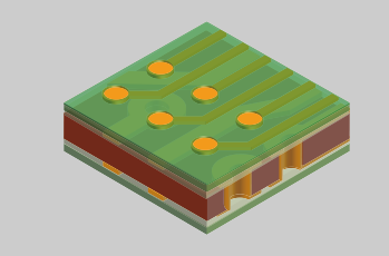
After applying solder resist, place solder bumps where LSI chips (die) will be mounted. After cutting into each pieces, inspect appearance and electric characteristics.
Applications
-
 Network device
(ASIC) -
 Server / PC
(CPU)
-
 AI Processor
 -
 Automotive
(Infotainment / ADAS)
-
 Home Game Console
(SoC) -
 Graphic Processing Unit
(GPU)
Product Lineup
-
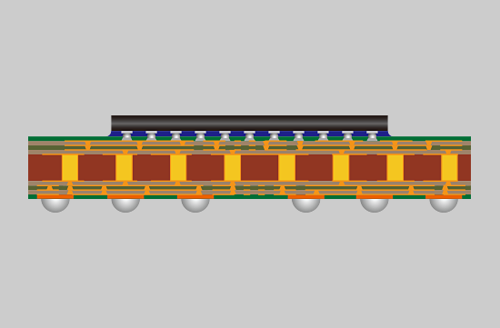 FC-BGA
 -
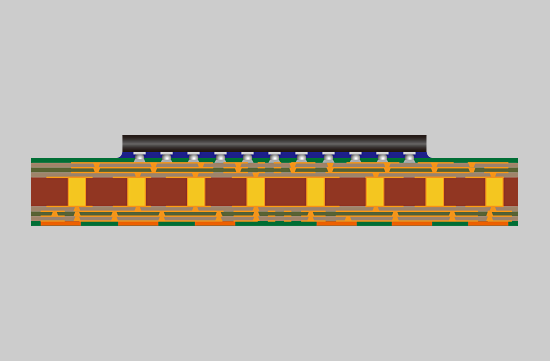 FC-LGA
-
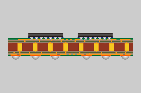 Multi-chip FC-BGA
 -
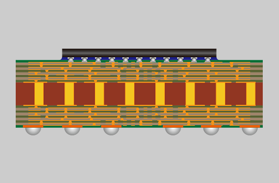 Ultra-multilayer FC-BGA
-
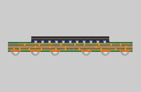 Coreless FC-BGA
 -
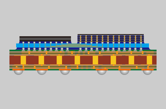 2.3/2.5D FC-BGA
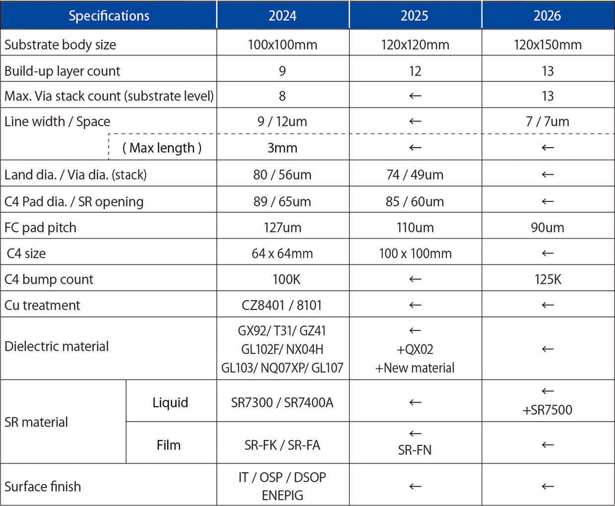
Roadmap
Buildup - Outer
Core
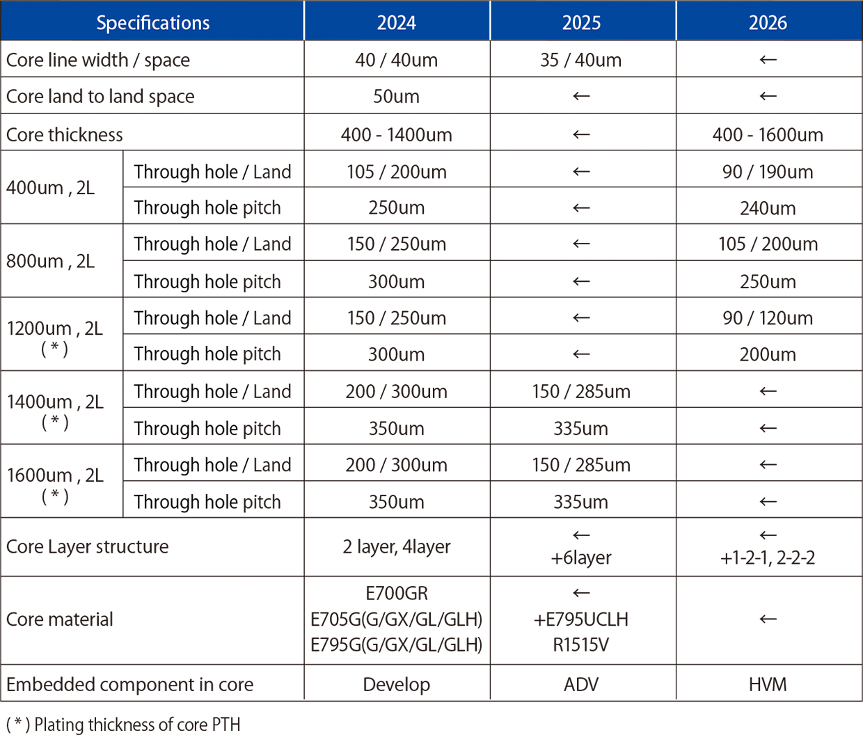
※ Please contact us individually about the materials for prototyping/evaluation.
Features
High-density Support
-

-
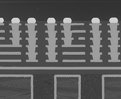 Hyper Build-up5 stack VIA
Land / Via = 85 / 60μm -
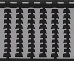 Structure of Via10 stack VIA
Land / Via = 100 / 60μmm -

Fine-pitch FC bump
-

-
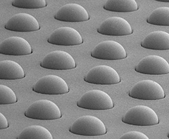 FC bumpPitch = 130μm
 -
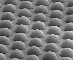 FC bumpPitch = 110μm
 -

SR DAM
Low copper roughness treatment
-
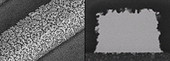 Ra:400-250nm
 -
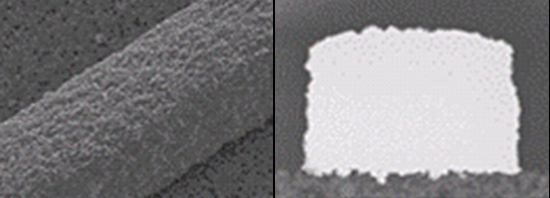 Ra:200-100nm
Higher Pin Account / Ultra Fine Wiring
-
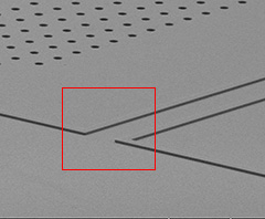
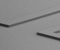
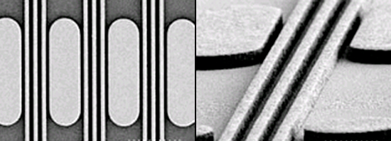 Fine Pitch Patterning (Semi Additive Process)Line / Space = 10 / 10μm
 -
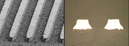 Fine Pitch Patterning (Subtractive Process)Line / Space = 30 / 30μm
High-resolution Resist pattern (Under Development)
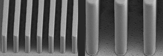
Materials for high-speed transmission
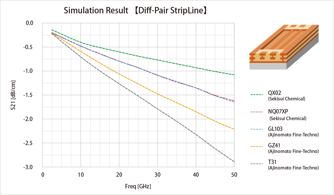
High-speed transmission build-up resin manufacturer
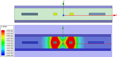
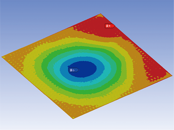
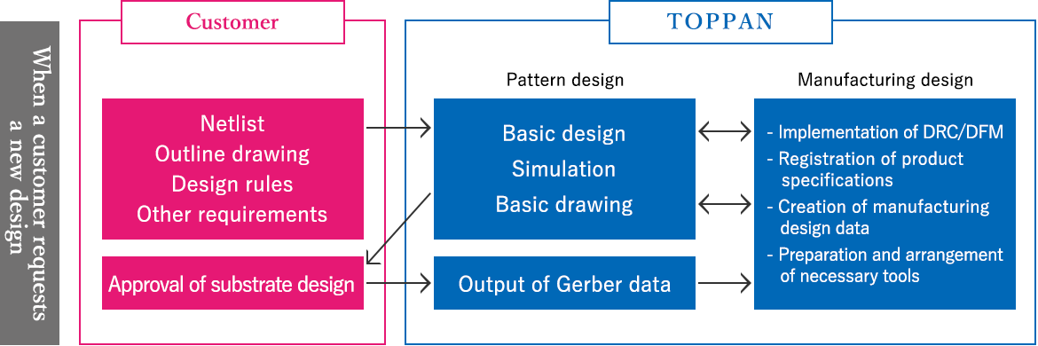
Support for design and simulation
Designing process flow
Simulation service
-
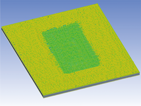
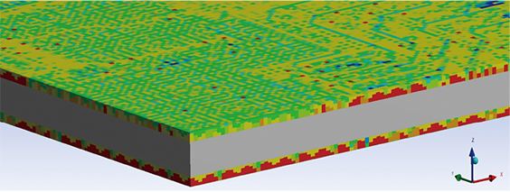
Heat transmission
analysis example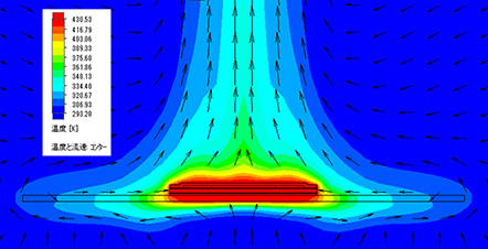
-
Electromagnetic
analysis example